2. BCU2002 Pinouts and Descriptions
The BCU2002 stands as a cutting-edge power management device designed for efficiency and adaptability across a range of applications. Its user-friendly design incorporates a wake-up trigger in the form of a user button, complemented by Power and Run/Error status LEDs for intuitive operational feedback. Boasting 4 relay outputs, 1 user button with an integrated LED, and microSD card support, the BCU2002 offers extensive input and output capabilities. The onboard Real-Time Clock (RTC) with a backup battery ensures accurate timekeeping, while its unique daisy-chain slave communication feature, supported by 1.5kV isolated RJ45 interfaces, allows seamless integration with up to 16 slave modules. With compatibility for various communication protocols like LiBat COM, JSON, Modbus RTU, Custom Canbus, and RS485, alongside support for 5V external current sensors, the BCU2002 ensures adaptability and precision.
Danger
Make sure all the connections done correctly and double check the cables. Think twice before plug into any connectors on BCU2002.
Fig.2.1: BCU2002, Board Pinout (TOP)
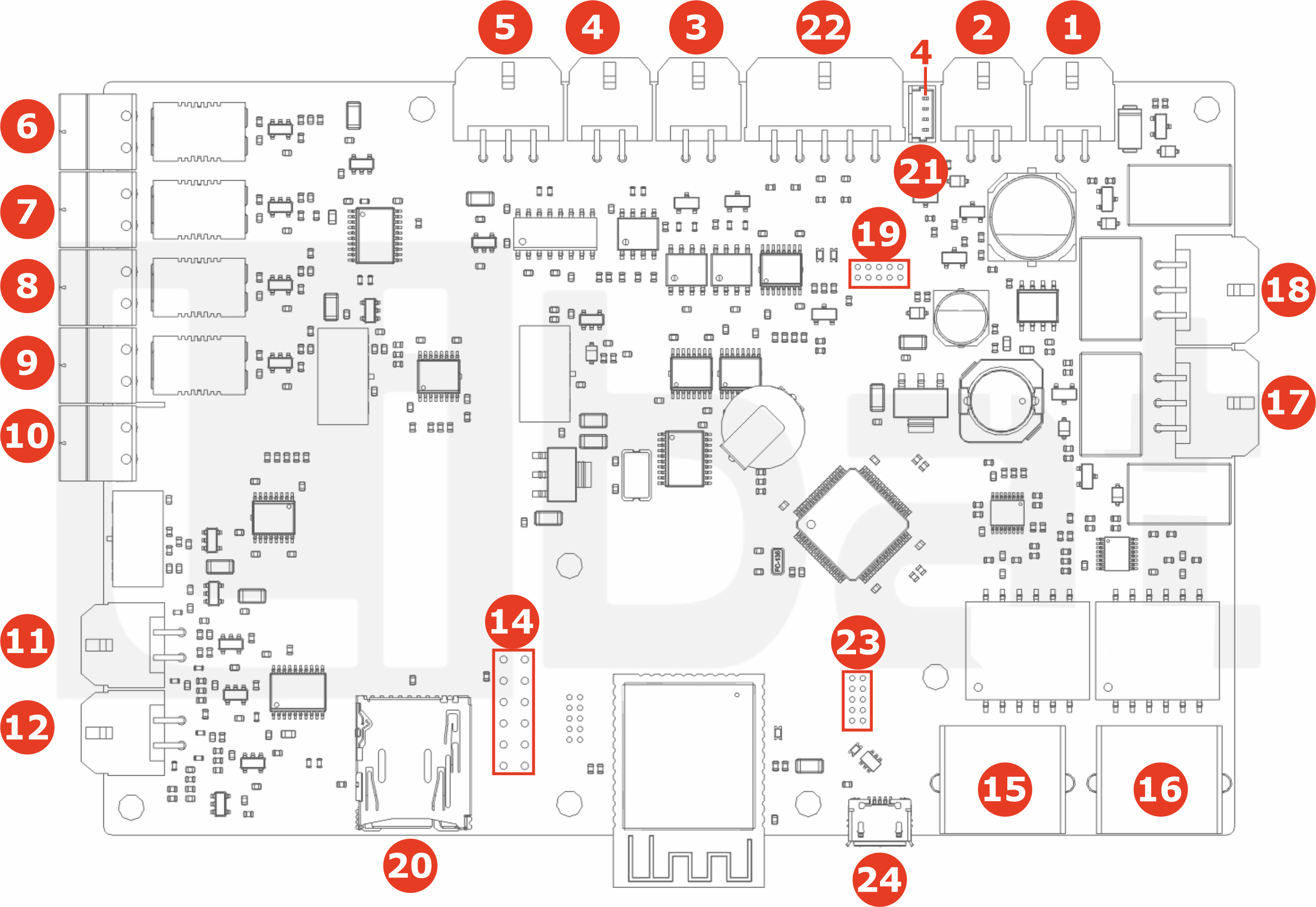
Fig.2.2: BCU2002, Board Pinout (BACK)
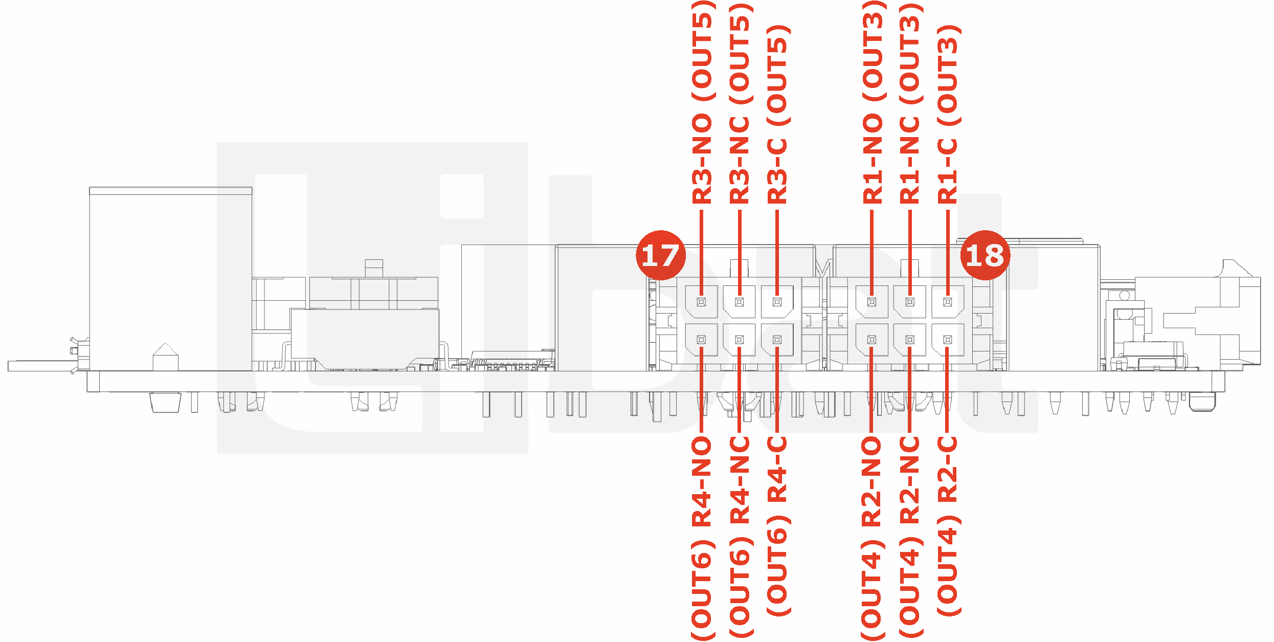
Fig.2.3: BCU2002, Board Pinout (FRONT)
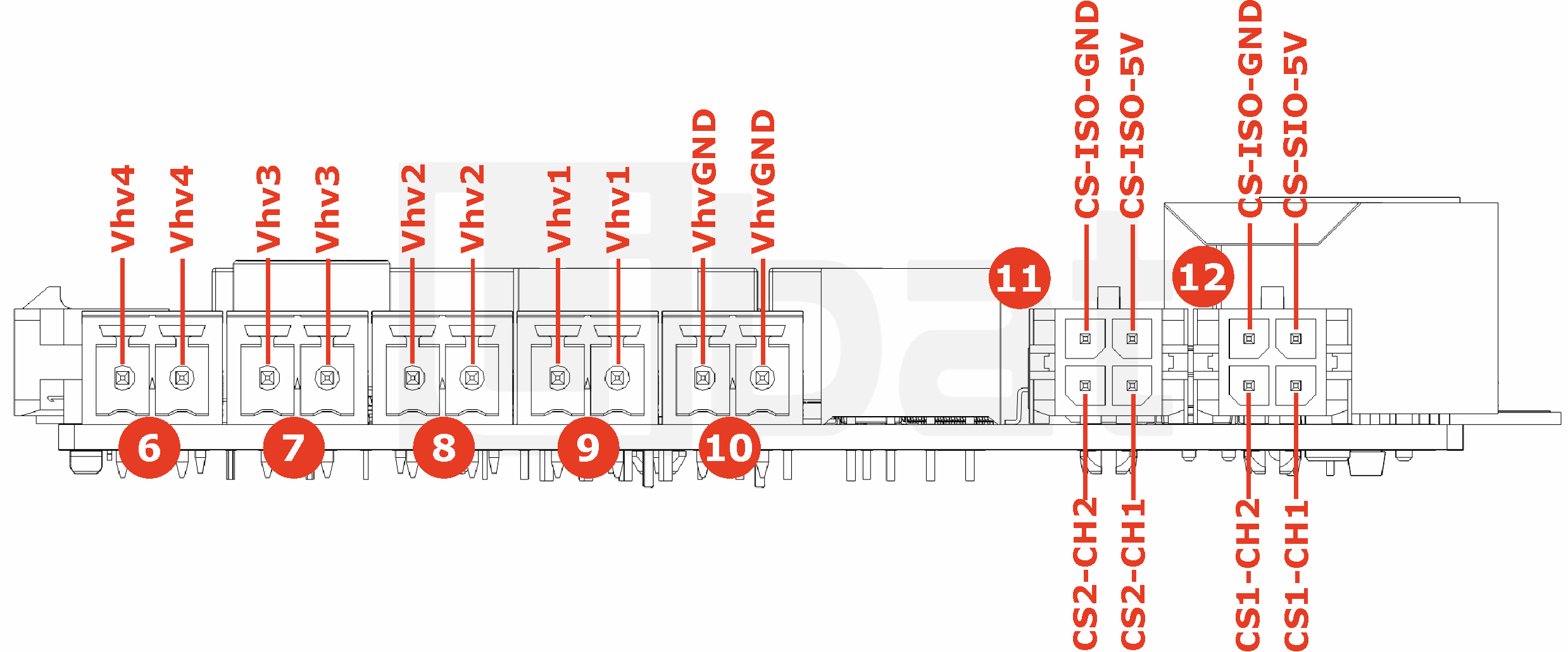
Fig.2.4: BCU2002, Board Pinout (LEFT)
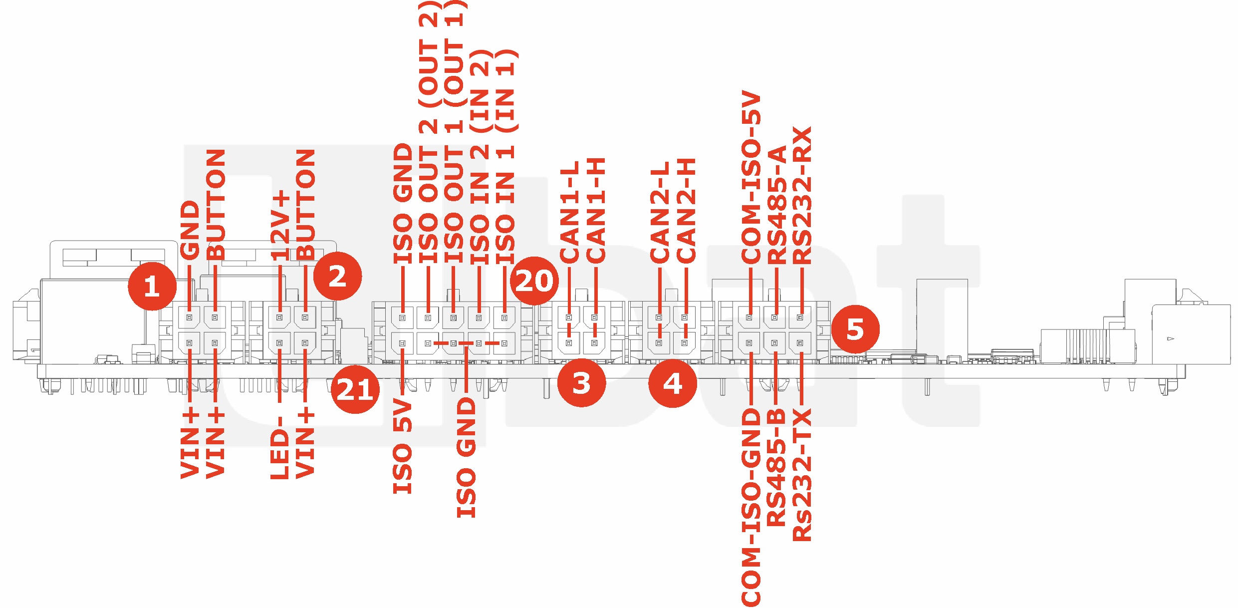
Fig.2.45: BCU2002, Board Pinout (RIGHT)
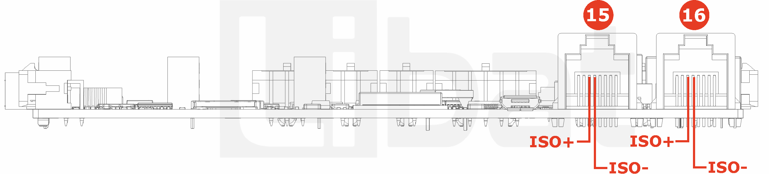
Table.2.1: Connector No#1 Descriptions
| Connector No. | Pin No. | Description (Refer the Fig.2.1 and Fig.2.4) |
|---|---|---|
| 1 | 1 | Board VIN+ (Board Main Power) |
| 1 | 2 | Board VIN+ Output |
| 1 | 3 | External Button Input |
| 1 | 4 | Board GND (Board Main Power) |
Table.2.2: Connector No#2 Descriptions
| Connector No. | Pin No. | Description (Refer the Fig.2.1 and Fig.2.4) |
|---|---|---|
| 2 | 1 | Board VIN+ Output |
| 2 | 2 | External Led GND Output |
| 2 | 3 | External Button Input |
| 2 | 4 | +12V Output |
Table.2.3: Connector No#3, #4 Descriptions
| Connector No. | Pin No. | Description (Refer the Fig.2.1 and Fig.2.4) |
|---|---|---|
| 3 | 1, 3 | CAN 2.0b CH1 High Pin |
| 3 | 2, 4 | CAN 2.0b CH1 Low Pin |
| 4 | 1, 3 | CAN 2.0b CH2 High Pin |
| 4 | 2, 4 | CAN 2.0b CH2 Low Pin |
Table.2.4: Connector No#5 Descriptions
| Connector No. | Pin No. | Description (Refer the Fig.2.1 and Fig.2.4) |
|---|---|---|
| 5 | 1 | RS232 No.0 Transmit Data (Service Port) |
| 5 | 2 | RS485 No.2 B Pin |
| 5 | 3 | ISO- GND |
| 5 | 4 | RS232 No.0 Receive Data (Service Port) |
| 5 | 5 | RS485 No.2 A Pin |
| 5 | 6 | ISO-5V Output |
Table.2.5: Connector No#6, #7, #8, #9, #10 Descriptions
| Connector No. | Pin No. | Description (ReferRefer the Fig.2.1 and Fig.2.3) |
|---|---|---|
| 6 | 1, 2 | High Voltage Measurement Positive Input CH4 (HVIN No#4 Assignment) |
| 7 | 1, 2 | High Voltage Measurement Positive Input CH3 (HVIN No#3 Assignment) |
| 8 | 1, 2 | High Voltage Measurement Positive Input CH2 (HVIN No#2 Assignment) |
| 9 | 1, 2 | High Voltage Measurement Positive Input CH1 (HVIN No#1 Assignment) |
| 10 | 1, 2 | High Voltage Measurement Block Common GND |
Table.2.6: Connector No#11 Descriptions
| Connector No. | Pin No. | Description (Refer the Fig.2.1 and Fig.2.3) |
|---|---|---|
| 11 | 1 | Current Sensor No#2 CH1 Sense Input |
| 11 | 2 | Current Sensor No#2 CH2 Sense Input |
| 11 | 3 | Current Sensor No#2 ISO 5V Output for Sensor Power |
| 11 | 4 | Current Sensor No#2 ISO GND Output for Sensor Power |
Table.2.7: Connector No#12 Descriptions
| Connector No. | Pin No. | Description (Refer the Fig.2.1 and Fig.2.3) |
|---|---|---|
| 12 | 1 | Current Sensor No#1 CH1 Sense Input |
| 12 | 2 | Current Sensor No#1 CH2 Sense Input |
| 12 | 3 | Current Sensor No#1 ISO 5V Output for Sensor Power |
| 12 | 4 | Current Sensor No#1 ISO GND Output for Sensor Power |
Table.2.8: Connector No#15 Descriptions
| Connector No. | Pin No. | Description (Refer the Fig.2.1 and Fig.2.5) |
|---|---|---|
| 15 | - | Isolated Daisy-Chain Connector No#1 (Standart RJ45) |
| 15 | 1,2,3,4,7,8 | Not Connected |
| 15 | 5 | Isolated daisy-chain communication port (ISO-) |
| 15 | 6 | Isolated daisy-chain communication port (ISO+) |
Table.2.9: Connector No#16 Descriptions
| Connector No. | Pin No. | Description (Refer the Fig.2.1 and Fig.2.5) |
|---|---|---|
| 16 | - | Isolated Daisy-Chain Connector No#2 (Standart RJ45) |
| 16 | 1,2,3,4,7,8 | Not Connected |
| 16 | 5 | Isolated daisy-chain communication port (ISO-) |
| 16 | 6 | Isolated daisy-chain communication port (ISO+) |
Table.2.10: Connector No#17 Descriptions
| Connector No. | Pin No. | Description (Refer the Fig.2.1 and Fig.2.2) |
|---|---|---|
| 17 | 1 | Relay Output No#4 Common Pin (OUT No#6 Assignment) |
| 17 | 2 | Relay Output No#4 Normally Closed Pin (OUT No#6 Assignment) |
| 17 | 3 | Relay Output No#4 Normally Open Pin (OUT No#6 Assignment) |
| 17 | 4 | Relay Output No#3 Common Pin (OUT No#5 Assignment) |
| 17 | 5 | Relay Output No#3 Normally Closed Pin (OUT No#5 Assignment) |
| 17 | 6 | Relay Output No#3 Normally Open Pin (OUT No#5 Assignment) |
Table.2.11: Connector No#18 Descriptions
| Connector No. | Pin No. | Description (Refer the Fig.2.1 and Fig.2.2) |
|---|---|---|
| 18 | 1 | Relay Output No#2 Common Pin (OUT No#4 Assignment) |
| 18 | 2 | Relay Output No#2 Normally Closed Pin (OUT No#4 Assignment) |
| 18 | 3 | Relay Output No#2 Normally Open Pin (OUT No#4 Assignment) |
| 18 | 4 | Relay Output No#1 Common Pin (OUT No#3 Assignment) |
| 18 | 5 | Relay Output No#1 Normally Closed Pin (OUT No#3 Assignment) |
| 18 | 6 | Relay Output No#1 Normally Open Pin (OUT No#3 Assignment) |
Table.2.12: Connector No#14, #20 Descriptions
| Connector No. | Pin No. | Description (Refer the Fig.2.1 and Fig.2.4) |
|---|---|---|
| 14 | - | Port for LiBat Extension Board |
| 20 | - | Micro SD Card Connector (Push-Push) |
| 24 | - | Micro USB Connector |
Table.2.13: Connector No#21 Descriptions
| Connector No. | Pin No. | Description (Refer the Fig.2.1) |
|---|---|---|
| 21 | 1 | Button Input (Battery Voltage) |
| 21 | 2 | Button Input |
| 21 | 3 | LED + |
| 21 | 4 | LED - |
Table.2.14: Connector No#21 Descriptions
| Connector No. | Pin No. | Description (Refer the Fig.2.1) |
|---|---|---|
| 22 | 1, 3, 5, 7, 10 | ISO GND |
| 22 | 2 | Isolated Input 1 (IN No#1 Assignment) |
| 22 | 4 | Isolated Input 2 (IN No#2 Assignment) |
| 22 | 6 | Isolated OUT 1 (OUT No#1 Assignment) |
| 22 | 8 | Isolated OUT 2 (OUT No#2 Assignment) |
| 22 | 9 | Isolated 5V supply (50mA) |